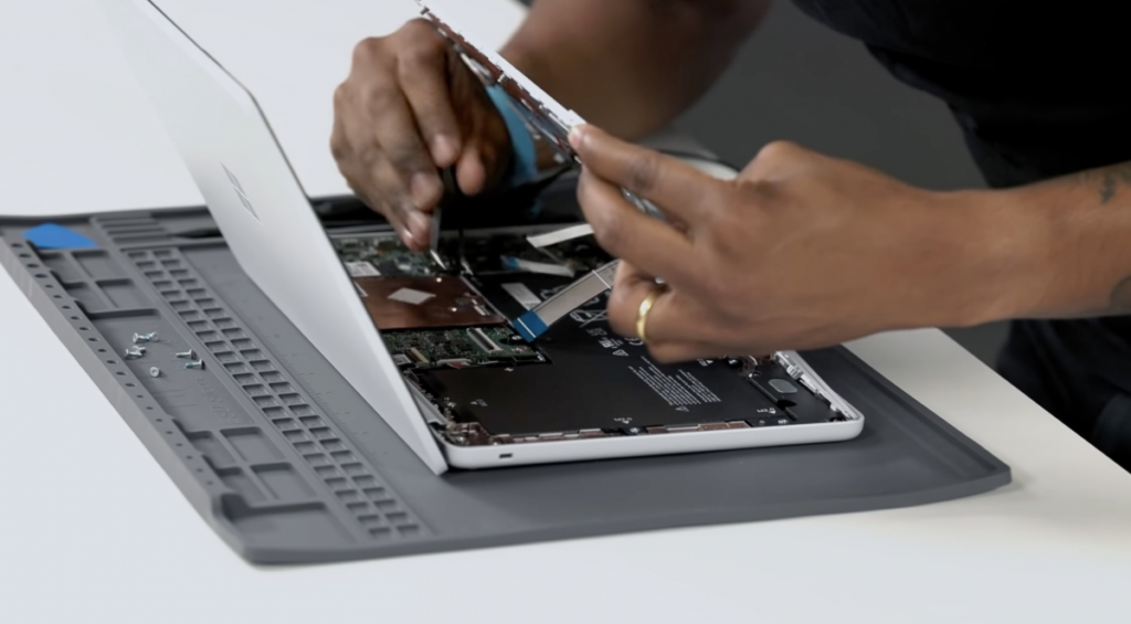


The evolution of 3D semiconductor packaging has unlocked new levels of performance, efficiency and miniaturization, but it has also introduced complex metrology challenges. Unlike traditional planar chips, 3D-stacked architectures require multi-layer alignment, defect detection at various depths and precise electrical connectivity. Without advanced metrology solutions, manufacturers risk reduced yield, performance inconsistencies and higher production costs. Erik Hosler, an expert in semiconductor metrology and process control, underscores that as packaging complexity increases, so must the precision and sophistication of metrology tools to maintain production efficiency and reliability.
The Metrology Challenges of 3D Integration
Unlike conventional semiconductor fabrication, where inspections primarily focus on the wafer surface, 3D integration introduces unique challenges that require deeper, multi-layer analysis. Some of the primary metrology concerns include:
Bonding and Alignment Accuracy – In 3D stacking, precise bonding between layers is essential. Even the slightest misalignment at the nanometer level can disrupt electrical connectivity, leading to device failures. Advanced metrology tools must detect variations in height, offset and warpage with extreme precision.
Through-Silicon Via (TSV) Inspection—TSVs are essential for vertical electrical connections in 3D chips, but defects in etching, filling, or liner deposition can cause signal loss or failure. Metrology tools must ensure precise dimensions and detect voids or cracks in real-time. Advanced techniques like X-ray tomography and acoustic metrology help identify irregularities early, preventing costly defects.
Warpage and Stress Measurement – As chips become thinner and more densely packed, stress-related warpage becomes a growing concern. Manufacturers need metrology tools that monitor warpages in real time to prevent defects that could compromise functionality.
Multi-Layer Defect Detection – Unlike traditional wafers, where defects are visible on the surface, 3D chips require non-destructive inspection methods that can detect hidden irregularities within multiple layers without dismantling the device.
Emerging Metrology Solutions for Advanced Packaging
New advancements in optical, X-ray and AI-driven metrology are addressing these challenges, helping manufacturers refine semiconductor inspection processes:
X-ray and Acoustic Metrology—These nondestructive imaging techniques allow fabs to inspect buried layers and interconnect in 3D-stacked devices, ensuring bond integrity and identifying voids in TSVs.
Optical Coherence Tomography (OCT) – This high-resolution imaging method enables real-time internal structure analysis, helping detect voids, cracks and misalignments before final assembly.
AI-Driven Inspection – AI-enhanced metrology analyzes vast data sets faster than traditional methods, identifying defect patterns and process deviations with greater accuracy.
Erik Hosler points out, “AI-driven tools are not only improving current semiconductor processes but also driving the future of innovation,” emphasizing the transformative role of AI in advancing metrology capabilities.
The Future of Metrology in 3D Semiconductor Packaging
As 3D semiconductor integration becomes more advanced, metrology must continue evolving to keep pace with increasing complexity. Traditional inspection techniques alone are no longer sufficient. The future of metrology will depend on real-time, high-precision and non-destructive methodologies that enable fabs to inspect chips at every stage of production without slowing down the process.
By leveraging AI, optical advancements and non-destructive testing, semiconductor manufacturers can overcome the metrology challenges of 3D packaging, ensuring higher yields, enhanced performance and long-term reliability for the next generation of semiconductor devices.